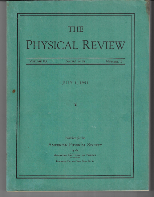
William Shockley, M. Sparks, and G.K. Teal, "p-n Junction transistors", in Physical Review, volume 83, no. 1, July 1, 1951, pp 151-163 in the issue of pp 1-248. Original wrappers. Very Good copy; there is a small brown blemish that extends in a diminishing capacity through the first 35pp in the extreme upper-right corner (visible on the cover and in the scan). $500
 Long quote from PBS "A Working Junction Transistor" from "Transistorized":
"Careful experiments led by a physicist in the group, Richard Haynes, helped. Haynes put electrodes on both sides of a thin germanium crystal and took very sensitive measurements of the size and speed of the current. Electricity definitely flowed straight through the crystal. That meant Shockley's vision of a new kind of transistor was theoretically possible.There was no doubt about it, point-contact transistors were fidgety. The transistors being made by Bell just didn't work the same way twice, and on top of that, they were noisy. While one lab at Bell was trying to improve those first type-A transistors, William Shockley was working on a whole different design that would eventually get rid of these problems. Early in 1948, Shockley conceived of a transistor that looked like a sandwich, with two layers of one type of semiconductor surrounding a second kind. This was a completely different setup which didn't have the shaky wires that made the point-contact transistors so hard to control. A working sandwich transistor would require that electricity travel straight across a crystal instead of around the surface. But Bardeen's theory about how the point-contact transistor worked said that electricity could only travel around the outside of a semiconductor crystal. In February of 1948, some tentative results in the Shockley lab suggested this might not be true. So the first thing Shockley had to do was determine just what was going on."
"But Haynes also discovered that the layer in the middle of the sandwich had to be very thin and very pure. The man who paved the way for growing the best crystals was Gordon Teal. He didn't work in Shockley's group, but he kept tabs on what was going on. He'd even been asked to provide crystals for the Solid State team upon occasion. Teal thought transistors should be built from a single crystal-as opposed to cutting a sliver from a larger ingot of many crystals. The boundaries between all the little crystals caused ruts that scattered the current, and Teal had heard of a way to build a large single crystal which wouldn't have all those crags. The method was to take a tiny seed crystal and dip it into the melted germanium. This was then pulled out ever so slowly, as a crystal formed like an icicle below the seed. Teal knew how to do it, but no one was interested. A number of institutions at the time, Bell included, had a bad habit of not trusting techniques that hadn't been devised at home. Shockley didn't think these single crystals were necessary at all. Jack Morton, head of the transistor-production group, said Teal should go ahead with the research, but didn't throw much support his way. Luckily, Teal did continue the research, working with engineer John Little. Three months later, in March of 1949, Shockley had to admit he'd been wrong. Current flowing across Teal's semiconductors could last up to one hundred times longer than it had in the old cut crystals."
With little support from management, Teal built the needed crystal-growing equipment himself, with help from mechanical engineer John Little and technician Ernest Buehler. Based on techniques developed in 1917 by the Polish chemist Jan Czochralski, he suspended a small "seed" crystal of germanium in a crucible of molten germanium and slowly withdrew it, forming a long, narrow, single crystal. Shockley later called this achievement "the most important scientific development in the semiconductor field in the early days."
"ALSO: "Employing this technique, Bell Labs chemist Morgan Sparks fabricated p-n junctions by dropping tiny pellets of impurities into the molten germanium during the crystal-growing process. In April 1950, he and Teal began adding two successive pellets into the melt, the first with a p-type impurity and the second n-type, forming n-p-n structures with a thin inner, or base, layer. A year later, such grown-junction transistors surpassed the best point-contact transistors in performance. Bell Labs announced this advance on July 4, 1951 in a press conference featuring Shockley."--"1951: First Grown-Junction Transistors Fabricated. Gordon Teal grows large single crystals of germanium and works with Morgan Sparks to fabricate an n-p-n junction transistor.", from computerhistory website.


Comments